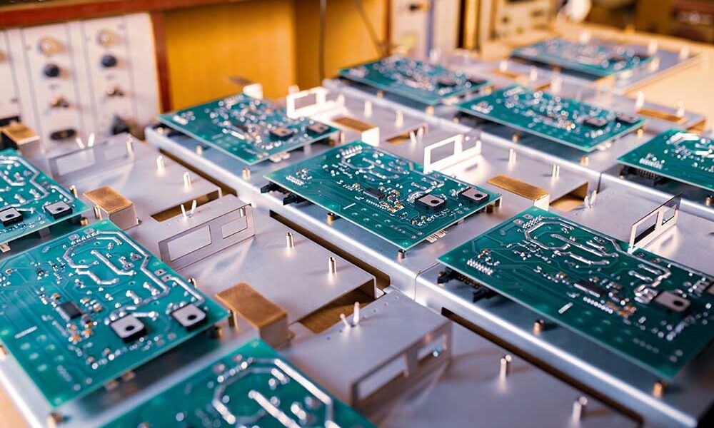
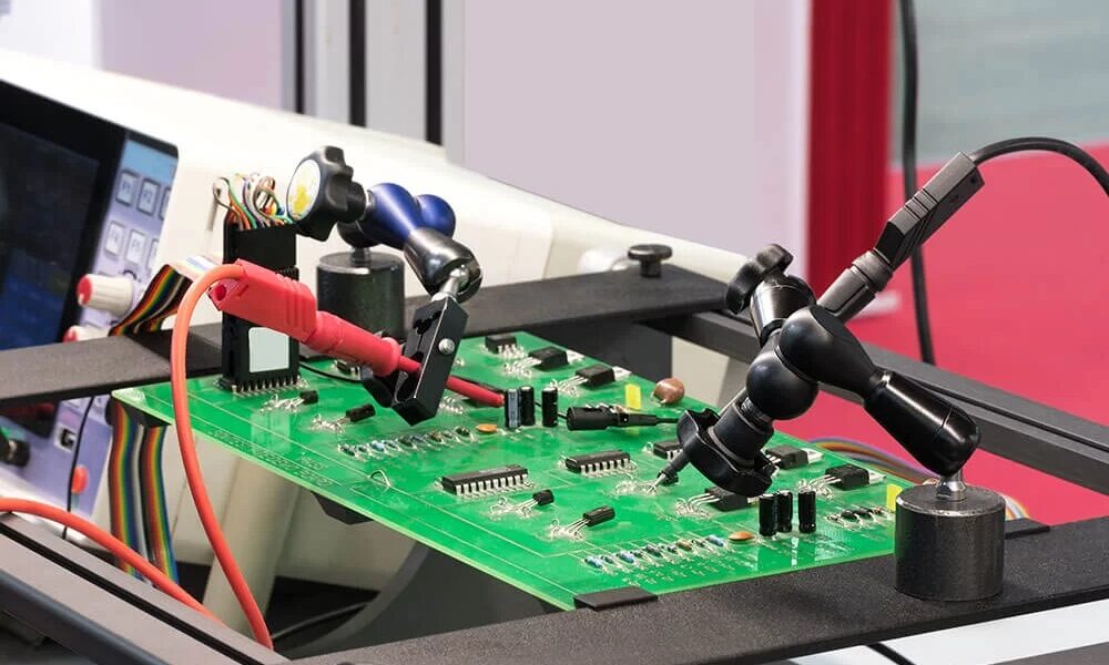
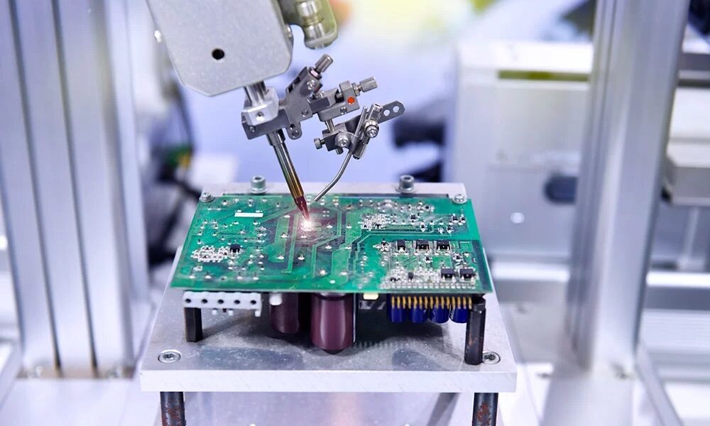
A Prototype PCB (Printed Circuit Board) is a fundamental component in the world of electronics and hardware development. It serves as a physical platform for designing, testing, and refining electronic circuits before they are mass-produced. Prototype PCBs play a crucial role in the product development cycle, enabling engineers and designers to validate their concepts, identify potential issues, and optimize the functionality and performance of their electronic devices.
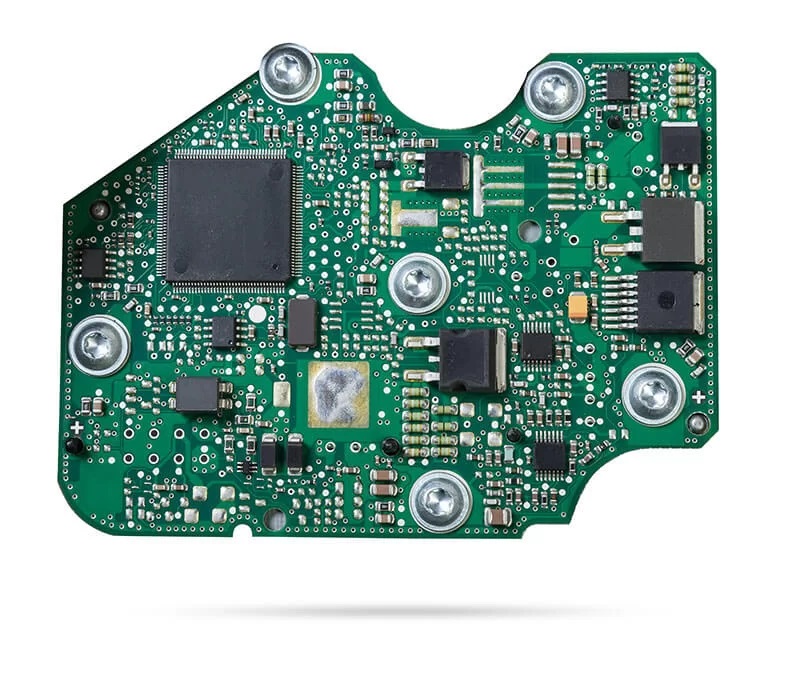
Features of Prototype PCBs
Design Iteration
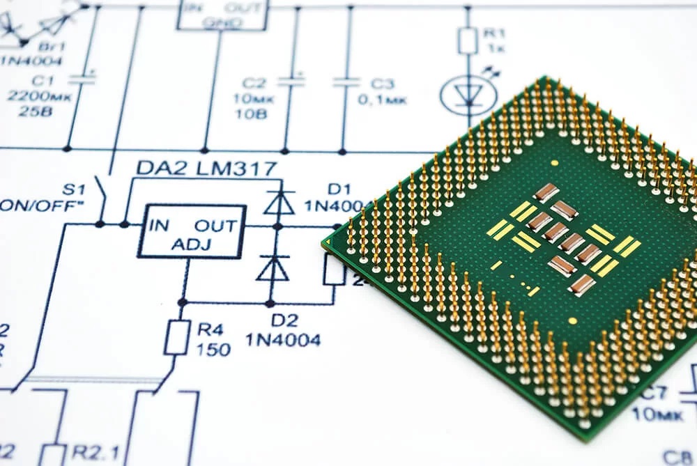
Before committing to a final design, engineers create a prototype PCB to validate their circuit schematics and layout. This iterative process allows them to identify and rectify design flaws, optimize component placement, and ensure proper signal integrity.
Component Mounting
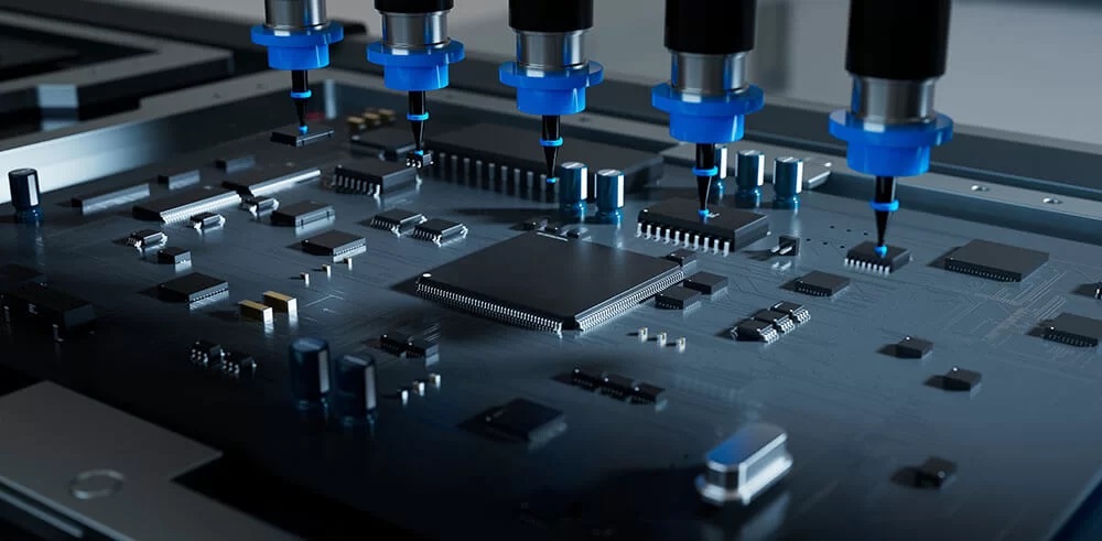
Prototype PCBs provide the necessary arrangement for mounting various electronic components such as resistors, capacitors, integrated circuits, connectors, and more. These components are soldered onto the board to form the functional circuit.
Customization
Prototype PCBs can be customized to match the specific requirements of a project. Designers can choose the size, shape, and layers of the board based on the complexity of the circuit and the intended application.
Testing and Debugging
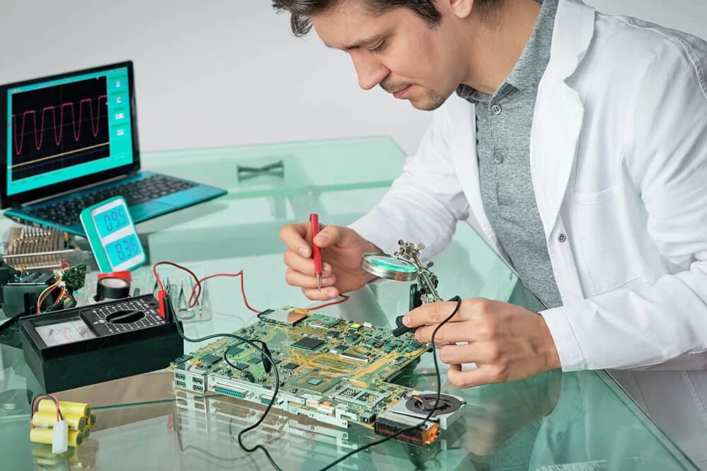
Once the components are soldered onto the board, engineers can test the circuit’s functionality, performance, and reliability. Debugging tools and test points on the prototype PCB aid in identifying issues and optimizing the design.
Rapid Prototyping
Advances in PCB fabrication technologies have led to the availability of rapid prototyping services, allowing designers to quickly iterate through multiple design versions. This accelerates the development process and reduces time-to-market for new products.
Proof of Concept
Prototype PCBs are often used to demonstrate the feasibility of a design concept to stakeholders, investors, or potential customers. A functional prototype can provide a tangible representation of the envisioned product.
Research and Development
In research and development environments, prototype PCBs are invaluable tools for experimenting with new ideas, exploring cutting-edge technologies, and pushing the boundaries of innovation.
Size and Form Factor Considerations
Depending on the application, prototype PCBs can vary in size and complexity. They can be single-sided, double-sided, or multi-layered, accommodating intricate circuits in a compact form factor.
Documentation
While prototype PCBs are primarily meant for testing and validation, proper documentation is still essential. Well-documented prototype designs can aid in transitioning to mass production by ensuring that the final design captures all necessary details.
Cost and Resources
While prototype PCBs provide a cost-effective means to develop and refine designs, they may involve higher costs compared to mass-produced PCBs. As such, careful consideration of budget and resources is crucial during the prototyping phase.
Prototype PCBs are indispensable tools in the electronics and hardware development process. They enable designers and engineers to transform abstract concepts into functional circuits, providing a tangible platform for experimentation, testing, and optimization. Whether for small-scale projects or large-scale innovations, prototype PCBs play a vital role in shaping the future of technology.
Prototype PCBs to large-scale PCB production
The importance of prototype PCBs before initiating large-scale PCB production cannot be overstated. Prototype PCBs serve as a critical bridge between the conceptual design phase and full-scale manufacturing. They offer numerous advantages that contribute to the success, efficiency, and cost-effectiveness of the overall PCB production process. Here’s why prototype PCBs are essential before embarking on large-scale production:
Design Validation
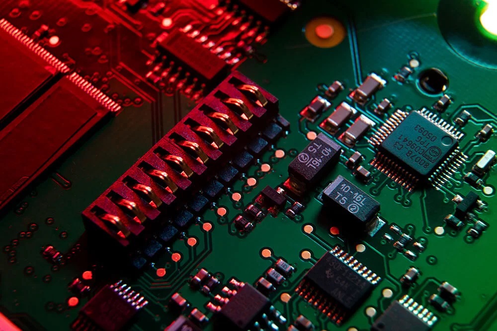
Prototype PCBs allow engineers and designers to validate their circuit designs and layouts in a real-world context. This step helps identify any design flaws, errors, or issues that might not have been apparent during the design phase. Catching and rectifying these problems at the prototype stage significantly reduces the likelihood of costly mistakes during mass production.
Functional Testing
Prototype PCBs provide an opportunity to test the functionality of the circuit under actual operating conditions. This testing can reveal potential performance bottlenecks, signal integrity issues, and other functional concerns. Addressing these problems early ensures that the final product meets its intended specifications.
Component Compatibility
During prototype PCB assembly, engineers can verify the compatibility of chosen components with the board layout and each other. This step helps ensure that components fit correctly, are properly soldered, and interact as intended.
Optimization and Refinement
Through prototype testing, designers can identify opportunities for optimization and refinement. This could involve adjusting component placement for better thermal management, signal routing for improved performance, or reducing unnecessary complexity to streamline the design.

Risk Mitigation
By producing a prototype PCB, potential risks associated with the final product can be assessed and mitigated before investing in mass production. This reduces the likelihood of costly rework or recalls due to unforeseen issues.
Cost Savings
While prototype PCB production involves costs, the investment pales in comparison to the potential expenses incurred from correcting errors or making design changes after large-scale production has begun. Addressing issues during the prototype phase is far more cost-effective.
Time-to-Market
Prototyping accelerates the product development cycle by allowing designers to iterate quickly. Rapidly testing and refining designs helps bring the product to market faster, which can be a crucial competitive advantage.
Supplier Relationships
The prototype PCB phase allows for vetting and building relationships with suppliers of components and materials. This early collaboration can lead to better pricing, availability, and quality assurance for the final production run.
Stakeholder Communication
Prototype PCBs provide a tangible platform for communicating design concepts to stakeholders, investors, or potential customers. Demonstrating a functional prototype can help garner support and feedback that contributes to the project’s success.
Process Optimization
The prototype PCB phase allows manufacturers to fine-tune their assembly and manufacturing processes, ensuring that they are well-prepared for large-scale production. Any challenges or bottlenecks can be identified and addressed before mass production begins.
Prototype PCBs play a vital role in mitigating risks, optimizing designs, and ensuring the successful transition from concept to large-scale production. They empower designers and engineers to validate their ideas, refine their designs, and address potential issues before significant resources are committed. Ultimately, prototype PCBs are an indispensable tool for achieving a smooth and efficient production process while delivering high-quality electronic products to the market.


